

Memory timing calculation is a critical aspect of optimizing system performance, particularly for enthusiasts and professionals working with high-performance computing setups. The timing parameters of a memory module, often represented as a series of numbers (e.g., CL16-18-18-36), directly influence data transfer efficiency and latency. This article explores the primary methods for calculating memory timings and their practical implications.
Core Concepts of Memory Timing
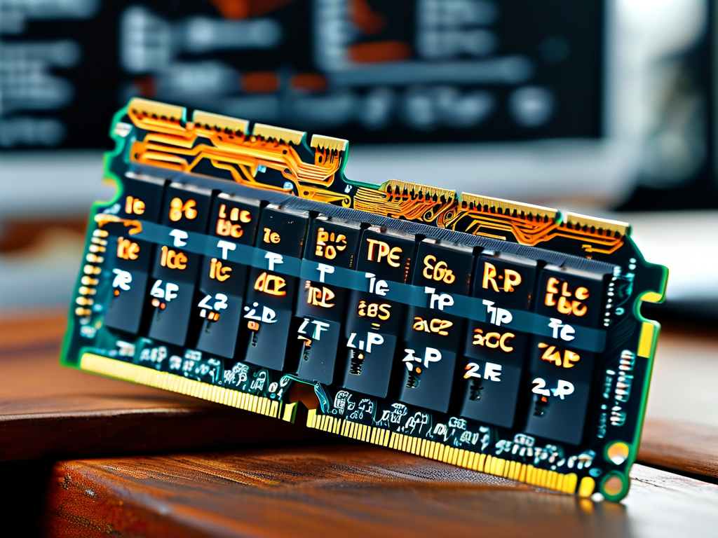
Memory timings refer to the delay intervals between specific operations performed by a memory module. These intervals are measured in clock cycles and include parameters such as CAS Latency (CL), Row Address to Column Address Delay (tRCD), Row Precharge Time (tRP), and Row Active Time (tRAS). Lower timings generally indicate faster performance but require higher-quality memory chips and stable hardware configurations.
Method 1: Frequency-to-Cycle Time Conversion
One foundational approach involves converting the memory module’s frequency into cycle time. For example, a DDR4 module operating at 3200 MHz has a clock cycle time of:
Cycle Time (ns) = 1 / (Frequency in GHz) = 1 / 3.2 ≈ 0.3125 ns This value helps calculate the actual latency for each timing parameter. CAS Latency (CL) is then determined by multiplying the cycle time by the CL value:
CL Latency = CL × Cycle Time For a CL16 module at 3200 MHz, this results in 16 × 0.3125 ns = 5 ns.
Method 2: Timing Ratio Analysis
Advanced users often analyze the ratios between timing parameters to identify bottlenecks. For instance, the relationship between tRCD and tRP affects how quickly a memory controller can switch between rows. A mismatched ratio may lead to suboptimal performance, even if individual timings appear tight. Tools like Thaiphoon Burner or DRAM Calculator for Ryzen automate this analysis by factoring in memory die type (e.g., Samsung B-die, Micron E-die) and motherboard capabilities.
Method 3: Latency-to-Bandwidth Tradeoff
Memory timing adjustments often involve balancing latency reduction against bandwidth limitations. Tightening timings may reduce latency but risk stability, while looser timings allow higher overclocks. A practical formula for evaluating this tradeoff is:

Effective Bandwidth = (Data Rate × Bus Width) / (1 + Latency Overhead) Here, latency overhead is derived from the cumulative impact of timing parameters. Overclocking tools like Intel XMP or AMD AMP profiles use similar logic to preset optimized configurations.
Real-World Applications
- Gaming PCs: Enthusiasts prioritize low CL values (e.g., CL14) to minimize frame time variance.
- Data Centers: Servers focus on tRAS and tRFC timings to ensure reliability under sustained workloads.
- Content Creation Workstations: Balanced timings with moderate overclocks maximize render speeds without instability.
Challenges in Timing Calculation
Modern DDR5 modules introduce complexities like on-die ECC and dual sub-channel architectures, which alter traditional timing calculation methods. Additionally, motherboard firmware and CPU memory controllers play a larger role in determining achievable timings. For example, AMD Ryzen’s Infinity Fabric clock syncs with memory speed, making timing adjustments interdependent with CPU settings.
Understanding memory timing calculation methods empowers users to tailor their systems for specific workloads. Whether through cycle-time conversions, ratio analysis, or latency-bandwidth optimization, each approach offers unique insights. As memory technologies evolve, staying informed about timing calculation principles remains essential for unlocking peak performance. Experimentation with benchmarking tools like AIDA64 or MemTest86 is recommended to validate stability after adjustments.