
In modern computing systems, memory performance plays a critical role in determining overall system efficiency. One often-overlooked aspect of memory optimization is the calculation of timing segmentation parameters, which govern how data is accessed and transferred within memory modules. This article delves into the foundational principles behind memory timing segmentation formulas, providing actionable insights for hardware engineers and enthusiasts.

Understanding Memory Timing Parameters
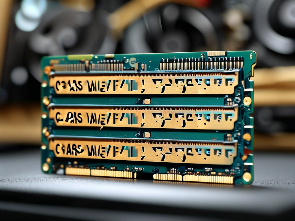
Memory timing refers to the sequence of delays between operations in dynamic random-access memory (DRAM). These delays are measured in clock cycles and are typically represented by values such as CL (CAS Latency), tRCD (RAS to CAS Delay), tRP (RAS Precharge Time), and tRAS (Active to Precharge Delay). Each parameter influences how quickly the memory controller can execute commands, directly affecting data throughput and latency.
The Core Calculation Framework
The memory timing segmentation formula is not a single universal equation but rather a set of interdependent calculations that vary based on memory type (e.g., DDR4, DDR5) and manufacturer specifications. A generalized approach involves three key steps:
-
Clock Cycle Conversion
Timing values are first converted from nanoseconds to clock cycles using the formula:Cycles = Timing (ns) × Frequency (GHz)For example, a CAS Latency of 14ns at 2GHz translates to 28 clock cycles.
-
Signal Propagation Adjustment
Physical constraints like PCB trace lengths and signal integrity require adding buffer cycles. This is often calculated as:Adjusted Cycles = Base Cycles + (Trace Delay × Frequency)Where trace delay is measured in picoseconds per millimeter.
-
Command Scheduling Optimization
Modern memory controllers use algorithms to interleave commands while respecting timing constraints. The segmented formula for command spacing becomes:tCMD = max(tRCD, tRP) + RoundTripDelay + Margin
Practical Implementation Example
Consider a DDR4-3200 module with CL=16, tRCD=18, and tRP=18. Using a 1.6GHz base clock (3200 MT/s effective):
- CAS Latency in nanoseconds: 16 / 1.6 = 10ns
- tRCD/tRP adjustment: Add 2 cycles for signal stabilization → 20 cycles (12.5ns)
- Total active time (tRAS): Typically CL + tRCD + 2 = 36 cycles (22.5ns)
Challenges in Real-World Applications
While these formulas provide a theoretical foundation, real-world implementations must account for:
- Voltage-temperature variations affecting signal integrity
- Manufacturing tolerances in memory chips
- Controller-specific scheduling quirks
Engineers often use iterative testing with tools like MemTest86 or manufacturer-provided RTL simulators to validate timing configurations.
Advanced Techniques
Cutting-edge optimization strategies include:
- Per-Rank Timing Calibration: Adjusting timings separately for dual-rank modules
- Adaptive Refresh Management: Dynamically modifying tRFC based on operating temperature
- Machine Learning Predictors: Using neural networks to forecast optimal timing margins
Industry Tools and Standards
JEDEC specifications provide baseline timing values, while third-party utilities like Thaiphoon Burner and Ryzen DRAM Calculator offer user-friendly interfaces for custom calculations. Open-source projects such as DRAMSim3 enable precise simulation of timing behaviors under different workloads.
Future Directions
Emerging memory technologies like LPDDR5X and HBM3 are introducing layered timing models where different banks operate with independent clocks. This necessitates segmented formulas with hierarchical constraints, pushing the boundaries of traditional calculation methods.
By mastering these timing segmentation principles, system designers can unlock hidden performance potential in memory subsystems while ensuring stability—a critical balance in applications ranging from gaming PCs to enterprise servers.