
Embedded systems development represents a specialized domain that merges hardware and software engineering to create efficient, resource-constrained solutions. Unlike traditional software projects, this process demands a meticulous approach to account for hardware limitations, real-time performance, and system reliability. Below is an in-depth exploration of the foundational workflow in low-level embedded development.

The journey begins with requirements analysis, where engineers define the system's purpose, performance benchmarks, and constraints. For instance, a medical device might require deterministic response times under 50ms, while an IoT sensor could prioritize ultra-low power consumption. This phase often involves collaboration with stakeholders to align technical specifications with practical use cases.
Next, hardware selection becomes critical. Developers choose microcontrollers (MCUs) or system-on-chip (SoC) components based on factors like clock speed, memory capacity, and peripheral support. A common trade-off occurs between ARM Cortex-M series processors for energy efficiency and RISC-V architectures for customization. Peripheral integration—such as ADC modules or wireless protocols—is validated through datasheets and reference designs.
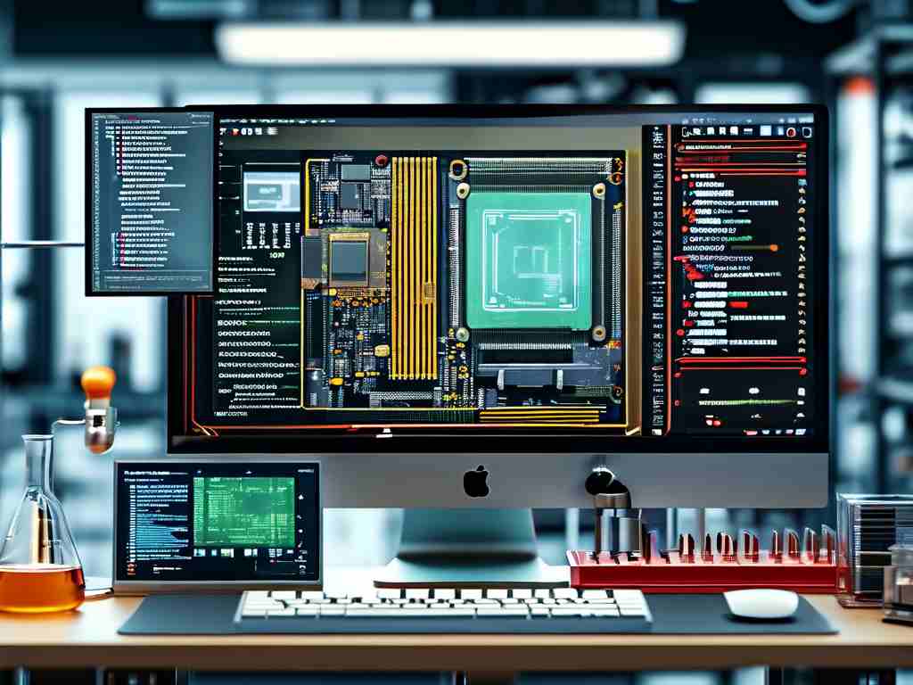
Once hardware is finalized, board bring-up commences. This involves PCB design, schematic verification, and initial firmware testing. Engineers often use breadboards or evaluation kits to prototype critical circuits. A basic firmware snippet for GPIO configuration might appear as:
void GPIO_Init() {
  RCC->AHB1ENR |= RCC_AHB1ENR_GPIOAEN;  // Enable GPIOA clock
  GPIOA->MODER &= ~GPIO_MODER_MODER5;    // Clear existing mode
  GPIOA->MODER |= GPIO_MODER_MODER5_0;   // Set PA5 as output
}
Simultaneously, toolchain setup is established. Developers configure cross-compilers, debug probes (like J-Link or ST-Link), and IDE environments such as Eclipse or VS Code with platform-specific plugins. Makefiles or CMake scripts automate build processes, ensuring compatibility with the target architecture.
The firmware development phase follows, typically structured in layered modules. Hardware abstraction layers (HAL) isolate MCU-specific operations, while middleware handles communication stacks (e.g., MQTT for IoT). Real-time operating systems (RTOS) like FreeRTOS or Zephyr may be implemented for task scheduling. Critical routines—such as interrupt service handlers (ISRs)—are optimized for speed:
void TIM2_IRQHandler() {
  if(TIM2->SR & TIM_SR_UIF) {
    TIM2->SR &= ~TIM_SR_UIF;  // Clear interrupt flag
    // Update PWM duty cycle here
  }
}
Testing and validation form a multi-stage checkpoint. Unit tests verify individual drivers using frameworks like Ceedling, while hardware-in-the-loop (HIL) testing evaluates system behavior under real-world conditions. Oscilloscopes and logic analyzers capture timing diagrams to confirm I2C or SPI transactions adhere to protocol standards.
Power optimization techniques are applied post-validation. Developers analyze current consumption with tools like Nordic Power Profiler, implementing sleep modes and clock gating. For battery-powered devices, dynamic voltage scaling might reduce MCU clock speeds during idle periods.
Finally, deployment and maintenance involve creating field-update mechanisms. Over-the-air (OTA) update systems using cryptographic signatures ensure secure firmware patches. Long-term reliability is monitored through error counters and watchdog timers that trigger system resets during hangs.
Throughout this workflow, version control (Git) and CI/CD pipelines maintain code integrity. A typical repository structure separates hardware schematics, firmware source, and test scripts into distinct branches.
Mastering embedded development requires balancing technical precision with creative problem-solving. By adhering to this structured workflow—while remaining adaptable to project-specific needs—teams can deliver robust embedded systems capable of operating reliably in diverse environments.