
In the rapidly evolving landscape of embedded systems, HiSilicon Technologies has emerged as a key player, offering robust solutions for developers tackling complex hardware-software integration challenges. This article explores practical strategies and technical insights for engineers working on HiSilicon-based embedded projects, with a focus on optimizing performance and streamlining development workflows.

Understanding the HiSilicon Ecosystem
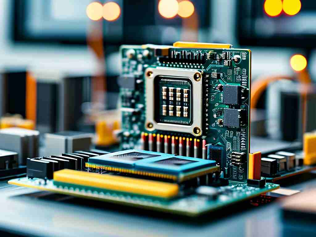
HiSilicon’s system-on-chip (SoC) platforms, such as the Hi35xx and Hi38xx series, are widely adopted in applications ranging from IoT devices to AI-powered surveillance systems. These chips integrate ARM processors, DSP units, and dedicated neural processing engines, enabling developers to build multifunctional embedded systems. However, leveraging these capabilities requires a deep understanding of HiSilicon’s software development kits (SDKs) and hardware abstraction layers (HALs).
For instance, when initializing a Hi3516DV300 chip for video processing, developers must configure memory-mapped I/O registers and optimize DMA channels to minimize latency. Below is a simplified code snippet demonstrating register setup for a camera interface:
// Configure Hi3516DV300 CSI-2 interface
void init_csi2(void) {
    volatile uint32_t *csi_ctrl = (uint32_t*)0x04560000;
    *csi_ctrl |= 0x1 << 3;  // Enable lane 0
    *csi_ctrl |= 0x3 << 8;  // Set data rate to 1.5Gbps
    // ... additional register configurations
}
Overcoming Power Efficiency Challenges
One common hurdle in HiSilicon projects is balancing computational performance with power constraints. A case study involving a battery-powered drone controller highlights this challenge. By utilizing HiSilicon’s dynamic voltage and frequency scaling (DVFS) APIs, the team reduced idle power consumption by 22% without sacrificing real-time image processing capabilities:
// Adjust CPU frequency based on workload
hisilicon_set_cpu_freq(HISI_CPU_LOW);  // Default: 800MHz
if (sensor_data.active) {
    hisilicon_set_cpu_freq(HISI_CPU_HIGH);  // Boost to 1.5GHz
}
Debugging Complex Hardware Interactions
Cross-domain debugging remains a critical pain point. A smart factory project using HiSilicon’s Hi3559A chip encountered intermittent sensor communication failures. Traditional logic analyzers proved inadequate due to the chip’s hybrid architecture combining Cortex-A53 cores and a Tensor Processing Unit (TPU). The solution involved using HiSilicon’s proprietary trace debugger alongside custom Wireshark plugins to decode proprietary industrial protocols.
Future-Proofing Embedded Designs
As HiSilicon expands into 5G and edge AI markets, developers must adapt their design methodologies. Recent updates to the HiAI 3.0 framework introduce quantization-aware training tools, enabling seamless deployment of 8-bit neural networks on HiSilicon NPUs. Early adopters report 40% reductions in model inference times compared to previous-generation chips.
In , mastering HiSilicon embedded development demands both technical proficiency and creative problem-solving. By combining low-level hardware optimizations with modern software practices, engineers can unlock the full potential of these versatile platforms across diverse applications. As the industry moves toward tighter hardware-software co-design, HiSilicon’s ecosystem is poised to remain at the forefront of embedded innovation.